

| Specification Item | �� | Value | Tolerance | Remark(s): |
 |
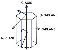
Standard Orientation | C-Plane | ��0.3�� | (0001) |
| Special Orientation | C+0.2��to A | ��0.1�� | on request | |
| Primary Flat Orientation | A-Plane | ��0.3�� | (11-20) | |
| Primary Flat Length | 16.0mm | ��1.0mm | �� | |
| Secondary Flat | �� | �� | on request | |
| Diameter | �� | 50.80mm | ��0.15mm | �� |
| Thickness(center point) | 330-430��m | ��25��m | �� | |
| Total Thickness Variation(TTV) | �� 15��m | �� | �� | |
| Local Thickness Variation(LTV) | �� 5��m,95�� | �� | 5mm x 5mm | |
| Bow | �� | ��20��m | �� | �� |
| Front Surface Roughness(Ra) | �� 5A | �� | MIL standard | |
| Backside Surface Roughness(Ra) | ��1.0��m | �� | ground | |
| Chips | �� | 3x��0.2mm | �� | max. |
| Wafer Edge Bevel | �� | ����150��m at 45�� | �� | �� |
| Cleanliness | �� | no stains and finger prints,ready for epi | �� | �� |
| Packaging | �� | cassettes of 25pcs or individually | �� | �� |
Li2B4O7
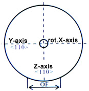
| Basic SAW Properties(45��rotated X-cut) | |||
| Propagation Direction: | Z-axis | ||
| EI.-Mech.Coupling Coefficient(K2): | 0.0 | ||
| Surface Wave Velocity: | 3401m/s | ||
| Group Delay Time Temp.Coefficient: | 0ppm/�� | ||
| Specification Item | �� | Value | Tolerance |
 |
Orientation | 45��rotated X-cut | ��0.25�� |
| Orientation Flat | perpendicular to Z-axis | ��0.25�� | |
| Orientation Flat Length | 22.0mm | ��0.20mm | |
| Secondary Flat Position | none/on request | �� | |
| Secondary Flat Length | none/on request | �� | |
| Diameter | �� | 76.20mm | ��0.30mm |
| Thickness(center point) | 350��m��500��m | ��30��m | |
| Total Thickness Variation(TTV) | �� 10��m | �� | |
| Local Thickness Variation(lTV)within 5mm x 5mm | �� 1.5��m | 95��(PLTV) | |
| Bow | �� | .-25��m��bow��+25��m | �� |
| Warp | �� | �� 50��m | �� |
| Front Surface Roughness(Ra) | �� 7A | (mirror polished) | |
| Backside Surface Roughness(Ra) | 0.2��m��0.5��m | (GC# 1200 lapped | |
Other specifications are available on request.
3"LiTaO3 (LT)Wafers
| Commmodity | Czochraiski("CZ")Grown Lithium Tantalate(Single Crystal,Single Domain,Congruent Composition������ | |||
| Orientation | 42��rot.Y-cut��0.25�� | 38.8��rot.Y-cut��0.25�� | 36��rot.Y-cut��0.25�� | X-cut��0.25�� |
| Diameter | 76.2mm��0.3mm | 76.2mm��0.3mm | 76.2mm��0.3mm | 76.2mm��0.3mm |
| Orientation Flat | 22mm��2mm | 22mm��2mm | 22mm��2mm | 22mm��2mm |
| �� | perpendicular toX��0.25�� | perpendicular toX��0.25�� | perpendicular toX��0.25�� | parallel to Y-112.2��0.25�� |
| Second Flat | 10mm��3mm | 10mm��3mm | 10mm��3mm | 10mm��3mm |
| �� | CW 90���0.5��from OF | CW 105���0.5��from OF | CW 120���0.5��from OF | CW 150���0.5��from OF |
| Thickness | 350��m��30��m | 350��m��30��m | 350��m��30��m | 350��m��30��m |
| �� | 500��m��30��m | 500��m��30��m | 500��m��30��m | 500��m��30��m |
| Propagating Surface | "+"-side,Ra��7A | "+"-side,Ra��7A | "+"-side,Ra��7A | "+"-side,Ra��7A |
| Wafer Backside | GC#1000 lapped & etched | GC#1000 lapped & etched | GC#1000 lapped & etched | GC#1000 lapped & etched |
| �� | 0.2��m��Ra��0.5��m | 0.2��m��Ra��0.5��m | 0.2��m��Ra��0.5��m | 0.2��m��Ra��0.5��m |
| TTV | �� 10��m | |||
| LTV | �� 1.5��m within an area of 5mm �� 5mm | |||
| PLTV | �� 95%(3mm from edge excluded | |||
| Bow | .-25 �� bow �� +25��m | |||
| Warp | ��50��m | |||
| Curie Temperature | 605�� �� 2�� | |||
4"LiTaO3 (LT)Wafers
| Commmodity | Czochraiski("CZ")Grown Lithium Tantalate(Single Crystal,Single Domain,Congruent Composition������ | |||
| Orientation | 42��rot.Y-cut��0.25�� | 38.8��rot.Y-cut��0.25�� | 36��rot.Y-cut��0.25�� | X-cut��0.25�� |
| Diameter | 100.0mm��0.5mm | 100.0mm��0.5mm | 100.0mm��0.5mm | 100.0mm��0.5mm |
| Orientation Flat | 32mm��2mm | 32mm��2mm | 32mm��2mm | 32mm��2mm |
| �� | perpendicular toX��0.25�� | perpendicular toX��0.25�� | perpendicular toX��0.25�� | parallel to Y-112.2��0.25�� |
| Second Flat | 13mm��3mm | 13mm��3mm | 13mm��3mm | 13mm��3mm |
| �� | CW 90���0.5��from OF | CW 105���0.5��from OF | CW 120���0.5��from OF | CW 150���0.5��from OF |
| Thickness | 350��m��30��m | 350��m��30��m | 350��m��30��m | 350��m��30��m |
| �� | 500��m��30��m | 500��m��30��m | 500��m��30��m | 500��m��30��m |
| Propagating Surface | "+"-side,Ra��7A | "+"-side,Ra��7A | "+"-side,Ra��7A | "+"-side,Ra��7A |
| Wafer Backside | GC#1000 lapped & etched | GC#1000 lapped & etched | GC#1000 lapped & etched | GC#1000 lapped & etched |
| �� | 0.2��m��Ra��0.5��m | 0.2��m��Ra��0.5��m | 0.2��m��Ra��0.5��m | 0.2��m��Ra��0.5��m |
| TTV | �� 12��m | |||
| LTV | �� 1.5��m within an area of 5mm �� 5mm | |||
| PLTV | �� 95%(3mm from edge excluded | |||
| Bow | .-30 �� bow �� +30��m | |||
| Warp | ��60��m | |||
| Curie Temperature | 605�� �� 2�� | |||
| Commmodity | Czochraiski("CZ")Grown Lithium Niobate(Single,Congruent) | �� | �� |
| Orientation | 64��rotated.Y-cut��0.25�� | 127.86��rot.Y-cut��0.25�� | X-cut��0.25�� |
| Diameter | 76.2mm��0.3mm | 76.2mm��0.3mm | 76.2mm��0.3mm |
| Orientation Flat | 22mm��2mm | 22mm��2mm | 22mm��2mm |
| �� | perpendicular toX��0.25�� | perpendicular toX��0.25�� | �� |
| Thickness | 350��m��30��m | 350��m��30��m | 350��m��30��m |
| �� | 500��m��30��m | 500��m��30��m | 500��m��30��m |
| Propagating Surface | "+"-side,Ra��7A | "+"-side,Ra��7A | "+"-side,Ra��7A |
| Wafer Backside | GC#1000 lapped & etched | GC#1000 lapped & etched | GC#1000 lapped & etched |
| �� | 0.2��m��Ra��0.5��m | 0.2��m��Ra��0.5��m | 0.2��m��Ra��0.5��m |
| TTV | �� 10��m | ||
| LTV | �� 1.5��m within an area of 5mm �� 5mm | ||
| PLTV | �� 95%(3mm from edge excluded | ||
| Bow | .-25 �� bow �� +25��m | ||
| Warp | ��50��m | ||
| Curie Temperature | 1142�� �� 2�� | ||
4"LiNbO3 (LN)Wafers
| Commmodity | Czochraiski("CZ")Grown Lithium Niobate(Single,Congruent) | �� | �� |
| Orientation | 64��rotated.Y-cut��0.25�� | 127.86��rot.Y-cut��0.25�� | X-cut��0.25�� |
| Diameter | 100.0mm��0.5mm | 100.0mm��0.5mm | 100.0mm��0.5mm |
| Orientation Flat | 32mm��2mm | 32mm��2mm | 32mm��2mm |
| �� | perpendicular toX��0.25�� | perpendicular toX��0.25�� | perpendicular to Z��0.25�� |
| Thickness | 350��m��30��m | 350��m��30��m | 350��m��30��m |
| �� | 500��m��30��m | 500��m��30��m | 500��m��30��m |
| Propagating Surface | "+"-side,Ra��7A | "+"-side,Ra��7A | "+"-side,Ra��7A |
| Wafer Backside | GC#1000 lapped & etched | GC#1000 lapped & etched | GC#1000 lapped & etched |
| �� | 0.2��m��Ra��0.5��m | 0.2��m��Ra��0.5��m | 0.2��m��Ra��0.5��m |
| TTV | �� 12��m | ||
| LTV | �� 1.5��m within an area of 5mm �� 5mm | ||
| PLTV | �� 95%(3mm from edge excluded | ||
| Bow | .-30 �� bow �� +30��m | ||
| Warp | ��60��m | ||
| Curie Temperature | 1142�� �� 2�� | ||